
 MENU
MENU 

Open-source hardware: a growing movement to democratize IC design
The University of Michigan is part of a growing movement to make integrated circuits (IC) or chip design more accessible by providing open-source process design kits (PDKs), EDA tools, and building blocks. Chips developed from these design kits are now also invited to be fabricated at no cost to the developer thanks to a cooperative research agreement between the U.S. Department of Commerce’s National Institute of Standards and Technology (NIST) and Google.

“The goal is to lower the barrier and access to silicon,” said research scientist Mehdi Saligane, “and at the same time allow people to push the limit of what can be done.”
Saligane has been at the forefront of open-source chip design and provides a unique perspective on the program, which is currently funding his own research. Parts of Saligane’s research focus on cloud-based data-driven circuit optimization, which leverages modern software practices into chip design. Open-source EDA tools and PDKs are key to his research since Saligane’s group is able to run in parallel thousands of designs on Google’s Cloud Platform. Such an experiment is only imaginable if the end-to-end toolchain requires no license. Saligane adds: “the open-source chip design ecosystem encourages reproducibility and reuse, which leads to great educational content available online to everyone.”
Right now, at top research institutions such as the University of Michigan, it would be nearly impossible to mimic the highly complex design work that goes into their state-of-the-art chips. Such institutions are also more likely to be able to pay the high cost of fabrication to test the viability of their designs in an actual prototype.
Saligane says such research is critical and will not be impacted by a parallel approach to encourage and enable more participation in the design process.
It’s an exciting time for anyone who wants to learn chip design.
Mehdi Saligane
One of the benefits of an open source PDK, explained Saligane and Google software engineer Tim Ansell in this invited paper, is to facilitate the development of the accompanying electronic design automation (EDA) tooling and open source register transfer language (RTL) by a greater number of individuals. Google has been a strong advocate for letting everyone see under the hood what goes into a hardware design, what they call “open source silicon.”
Through Google’s open-source initiative, a researcher can adapt an open-source PDK, work with a variety of software experts on the tooling, and then have the final design fabricated at no cost by the SkyWater Technology semiconductor foundry. The only requirement is that the final PDK is made available to the public and be compatible with their 130 nm-CMOS process. Global Foundries also released open-source PDKs and offers a 180 nm-CMOS process at no cost to open-source chip innovators.
The potential savings in fabrication costs to researchers can reach hundreds of thousands of dollars.
The NIST and Google cooperative research agreement builds on the Google open-source initiative to include nanofabrication research by developing additional wafers and test structures for nanofabrication research.
The greatest expected impact will be on individual researchers in regions that are underrepresented in chip design, as well as small and/or startup companies. There has even been a name given to the difficulties experienced by many small companies: the tech-transfer valley of death, which refers to the time period between government and sustainable private support as technology moves from academia to the marketplace.
“By creating a new and affordable domestic supply of chips for research and development, this collaboration aims to unleash the innovative potential of researchers and startups across the nation,” said Laurie E. Locascio, Under Secretary of Commerce for Standards and Technology and NIST Director, in an agency news release.
Saligane likens what is happening in the world of chip design with the long-standing practice of free, open-source software. Free software has been a component of the software industry throughout its history, beginning as early as the 1950s. It is a term used to describe software that is completely open to the public, making it possible for individuals who had nothing to do with the creation of the code to modify it for their own purposes.
WordPress is a good example of open-source software. It is free to users and can be easily modified by those with programming ability. Software aficionados are familiar with the open-source software known as the GNU operating system, developed in the early 1980s in opposition to the growing trend of commercialized software. Free software has always existed alongside proprietary software, such as Windows or Photoshop. Google offers the free equivalent of Microsoft Office with its Google Docs.
In recent years, a movement has begun among hardware developers to offer the same access to source material relating to chip design. The IEEE Solid-State Circuits Society (SSCS), for example, established the Platform for IC Design Outreach (PICO) program in 2021 with the goal of “working with the rapidly growing open-source community to help accelerate the construction of the required ecosystem.”
Building on the program’s success, the SSCS established a new technical committee a year later dedicated to the open-source ecosystem. One of the committee’s first activities, led by Saligane and Prof. Boris Murmann (Stanford), was to initiate a Code-a-Chip competition. Among the international group of winners is undergraduate student Ali Hammoud, with the project “OpenFASoC: Digital LDO Generator.” Hammoud will present his design at the 2023 International Solid-State Circuits Conference.
The open-source hardware movement is thriving and revolutionizing the semiconductor scene and practices.
Dennis Sylvester
As a final example of the expanding popularity of open-source hardware, just this past September, a workshop dedicated to open-source multi-project wafers (MPWs), where multiple chip projects can be fabricated on the same wafer, was held at the co-located ESSDERC (European Solid-State Device Research Conference) and ESSCIRC (European Solid-State Circuits Conference) conferences. The workshop, coming one year after the release of the Skywater 130nm PDK, was chaired by Dennis Sylvester, Edward S. Davidson Collegiate Professor of ECE.
“With over 200+ ICs already taped out and thousands of chips expected this coming year, the open-source hardware movement is thriving and revolutionizing the semiconductor scene and practices,” stated Sylvester in the workshop.
Saligane presented a talk at this workshop, as did his close collaborator and long-time advocate for open source hardware, Tim Ansell, a software engineer at Google, and Michigan alumnus Matt Guthaus (BSE MSE Ph.D. EE ‘98 ‘00 ‘06), currently a professor of computer science and engineering at UC Santa Cruz.
This open-source hardware movement has become even more visible in light of the CHIPS ACT.
“I think it’s disruptive,” said Saligane. “There are a lot of behaviors in the hardware world that are changing right now and adopting more of the software mindset.”
That mindset, says Saligane, places a high premium on iteration – something that is actively minimized in chip design because of the high cost of production. If fabricating your chip design is going to cost in the neighborhood of $300K, you’re going to want that design to be as close to perfect as possible. But if it’s going to be free – you might experiment more. And, of course, it opens up the process to a much broader community of researchers.
As an early example of what can be done with open-source silicon, researchers at Michigan collaborated with Google and Efabless to develop an open-source, autonomously generated design for an autonomous temperature sensor. The design was fabricated by SkyWater as part of the first group of projects in the new Google-SkyWater 130nm experiment. Led by Saligane, the design benefited from the participation of Professors David Blaauw and Dennis Sylvester, the core team behind the Michigan Micro Mote, a millimeter-scale computing system that can be adapted for a variety of sensing applications.
The fabricated chip has been distributed to other researchers to test yet another aspect of reproducibility, namely, whether an open-source fabricated chip will perform the same in different environments. Because these are physical devices, there’s more room for variability compared to using open-source software or algorithms.
“In the software community, I can grab their code and know that it will perform exactly the same,” said Sylvester. “We don’t have that in hardware, but this is a movement in that direction, and I find that exciting.”
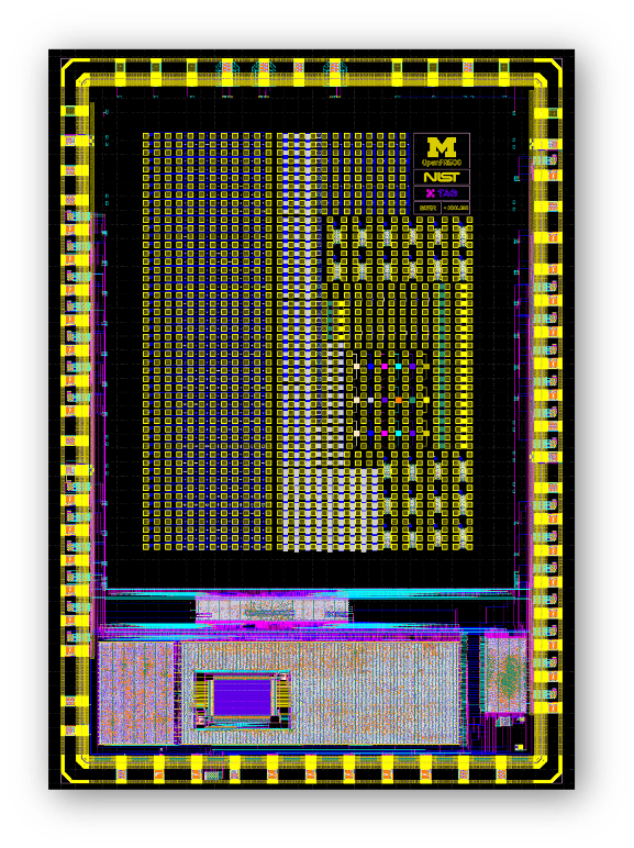
Saligane continued to partner with NIST in subsequent open-source designs, which resulted in one of the first successful chips using Google’s open multi-project wafer (MPW) program. This chip, called simply MPW-5, was based on a new open-source tool called openFASOC, short for Open-Source Fully Autonomous System-on-Chip. OpenFASOC, developed by Saligane and a team of researchers, including Sylvester, is the open-source corollary to FaSOC, a project led by Prof. David Wentzloff, with collaborators at the University of Virginia and ARM.
The MPW-5 chip was designed to meet the emerging needs of the nanofabrication community, says Saligane, namely easy integration and easy benchmarking. Featured in Google’s Open Source Blog, the MPW-5 chip took less than two months to design and was among the first open-source chip designs of its kind.
“This project involves designing many test structures used for the basic characterization of nanoelectronic devices. Research into such integrated circuits is important for developing new families of test structures for university researchers,” said Brian Hoskins, a research scientist at NIST.
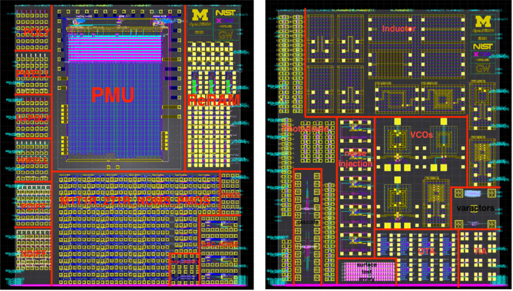
The MPW-5 was quickly followed by successful designs of increasing complexity. The most recently fabricated chip, MPW-7, includes 5 different photodiodes with access circuitry, VCOs, and inductors. Collaborators on these designs included faculty at George Washington University and Brown University.
“This shows the progress of an open-source tool in an open-source community,” said Saligane. “Everyone is iterating on their designs and doing things that are much more complicated.”
Perhaps an even more remarkable sign of the possibilities inherent in open source design is that the layout used for the VCO in MPW-7 was designed by high school students, with the assistance of Saligane’s doctoral students, Ming-Hung Chen and Anhang Li.
Another benefit to open source PDKs has to do with security. The very real problem of nefarious hacks to a printed circuit board has been described in this IEEE Spectrum article and elsewhere.
“With open source tools,” says Saligane, “you can audit the code and see exactly what you have on your chip, which gives you control over the toolchain.”
An important program initially funded by the government to facilitate open-source chip design is known as OpenROAD. Led by Prof. Andrew Khang at UCSD, with participation from Sylvester (co-PI), Blaauw, and Ronald Dreslinski, the OpenROAD project was initiated to provide open-source semiconductor design automation tools, which take the place of more traditional tools provided by companies like Cadence and Synopsys. The cost savings are dramatic.
“If I’m a guy in my garage,” said Sylvester, “I can’t afford to pay millions of dollars for licensed software tools.”
Finally, in yet another effort, the Center for Applications Driving Architectures, led by Professor Valeria Bertacco, is developing a “plug-and-play” modular approach to hardware design that aims to make it more accessible to a larger pool of talent. Launched in 2018 with $32 million, it is currently funded through a government-industry consortium and includes 21 faculty members and 130 graduate students from 11 universities.
In summary, open-source chip design has reached a tipping point in terms of research activity and funding, thanks to the government and industry supporting the efforts of open-source evangelists.
“The involvement of NIST and Google, and now the CHIPS Act, is catalyzing what’s happening in the world of open-source IC design and semiconductor nanofabrication,” said Saligane. “It’s an exciting time for anyone who wants to learn chip design.”